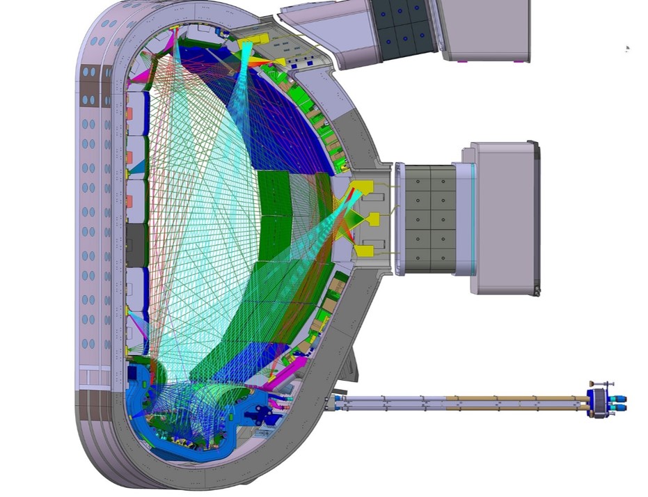
Looking into the chamber of the ITER tokamak, an array of over 100 sensors called bolometers will measure the x-ray, visible and infrared light shining out of the plasma. Information from the bolometers will be used by the ITER control systems to manage the energy within the plasma. The bolometer principle is simple.Radiation from the plasma is absorbed by the device and it heats up. The resistance is then measured to work out how much radiation has been absorbed. Operating conditions for the ITER bolometers will be tough. They must be robust enough to work in a vacuum, endure the constant bombardment of very energetic neutrons (14 MeV), operate at temperatures up to 400 °C, and provide reliable data readings within 1 millisecond .
Manufacture of bolometers at CSEM
The Centre Suisse d'Electronique et de Microtechnique (CSEM) in Neuchâtel has fabricated ~20 prototype bolometers for the European Agency Fusion for Energy (F4E) within their ITER technology development and long-term manufacturing pipeline. CSEM’s extensive knowledge of microelectromechanical systems (MEMS), sensor technologies, printed electronics, and surface coatings are well matched to the demands of this manufacturing project.
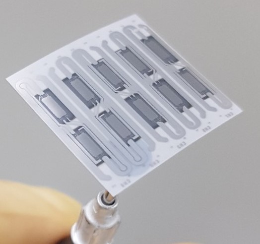
Each CSEM prototype bolometer is made of a thin wafer of ceramic, patterned on one side with a grid of metallic radiation absorbers, and on the other side with 5 circuits of thin film resistors.The 20 µm thick wafers (around one quarter the diameter of a human hair) are made of yttrium-stabilized zirconia (YSZ) ceramic and are extremely brittle.
On their own, the YSZ wafers are too fragile to be processed in the normal way, so engineers at CSEM have developed a special process to temporarily bond them onto carrier wafers that can be handled by different machines, together with the necessary tooling to manipulate and release the wafers. During the manufacturing sequence, the bonding and release of the YSZ wafer must be done twice, since processing is performed on both sides.
On the first side, the resistors are fabricated through sputtering of a platinum film, and its subsequent patterning by photolithography and dry etching. On the second side, absorbers are made by electrodeposition of gold in photoresist moulds, which requires the deposition of adhesion, barrier, and seeding layers.
Testing and performance
Stress management in the different layers during processing is critical for obtaining flat, crack-free devices and to ensure the long-term stability of the interfaces between the YSZ wafer and the gold absorbers.
The devices produced at CSEM have passed the stringent manufacturing and performance specifications set out by the ITER Organisations. Each bolometer was run through repeated thermal cycling tests from room temperature to 400 ºC to characterise the resistance response with temperature. Resistance variations across a full 5-channel sensor below 0.3% have been reached.
The prototype bolometers have been delivered to ITER and will now undergo neutron irradiation and further testing to evaluate their suitability for use within the tokamak environment.
Impact
CSEM has used this project to push MEMS manufacturing processes in Switzerland beyond standard MEMS activity, opening up new capability for the future.
CSEM has been able to show that its experts are very flexible in their approach to projects and that the organisation is well-placed to take on the challenges and complexities of working with unknown materials and unconventional product designs for small manufacturing runs.
Following the successful manufacture of the prototype bolometers, ITER has awarded CSEM a second project to develop a further technology connected with thin film devices.
About CSEM SA

The Centre Suisse d'Electronique et de Microtechnique (CSEM) is a Swiss private, non-profit research and technology organisation with over 35 years of experience of technology development and transfer to industry.
CSEM is committed to both applied and industry-commissioned R&D and supplies a broad range of markets including automotive, medical, machine tools, and space exploration. The organisation has long been renowned as one of Switzerland’s major research institutes in advanced microelectronics and microtechnology in the domain of precision manufacturing. With over 400 experts, CSEM is passionate about helping its partners achieve success by advancing digital technologies in the economy across a competitive and global industrial environment.

Marc-Alexandre Dubois
Senior Project Manager
CSEM
Neuchâtel, Switzerland